Circuits
This is a combination of knowledge that I have gained from ENGR 40M and EE 101A, both of which I took during summer quarter in 2025, and self-learning.
-
Phasors
- sin(x)=cos(x-90°)
-
Impedance
-
-
-
-
R - resistance
-
X - reactance
-
-
-
Admittance
-
G - conductance
-
B - susceptance
-
-
Capacitors have negative reactance and inductors have positive reactance
-
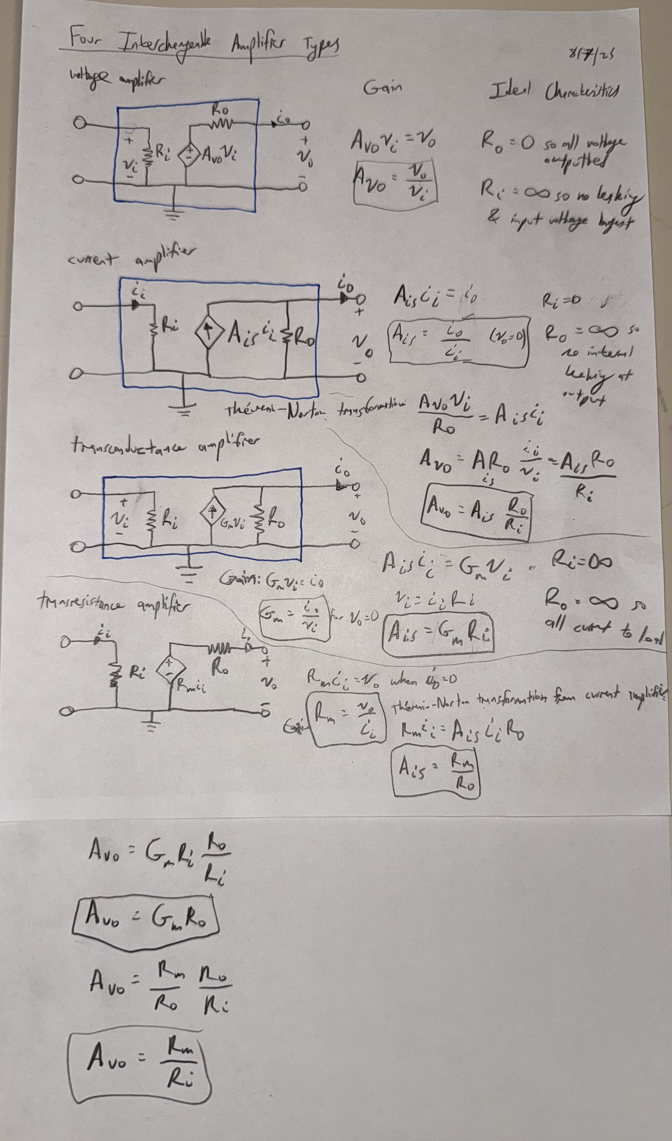
Four amplifier types
-
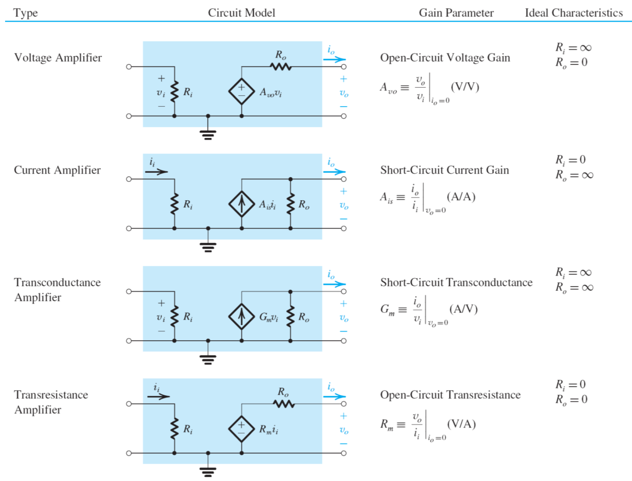
These four are equivalent. It's like VCVS, CCCS, VCCS, and CCVS. To remember, think of transconductance as having the gain of conductance so output current/input voltage and for transresistance as having the gain of resistance so output voltage/input current.
-
When there is an output voltage (for transresistance and voltage amplifier), it should be measured when the output terminals are open for there to be no current flowing through which would decrease .
-
When there is an output current, it should be measured when short-circuited so that none of the output current flows through (you get all the current flowing from the current source in )
-
trans - input and output of different types/at different places (voltage → current, current → voltage)
-
m in and is for "mutual" like in "mutual inductance" because the current and voltage are at separate ports (similar to trans-)
-
-
Equations for swapping between them using transformations (see derivation at [[#Four Interchangeable Amplifier Types]]):
-
Three parameters necessary for forming an amplifier: , and gain
-
Gains
-
/// - for the voltage/current source (no loads)
- intrinsic gain
-
/ - also considers and
- loaded gain
-
- everything, considers source resistance and multiple stages if applicable
- overall system gain
-
-
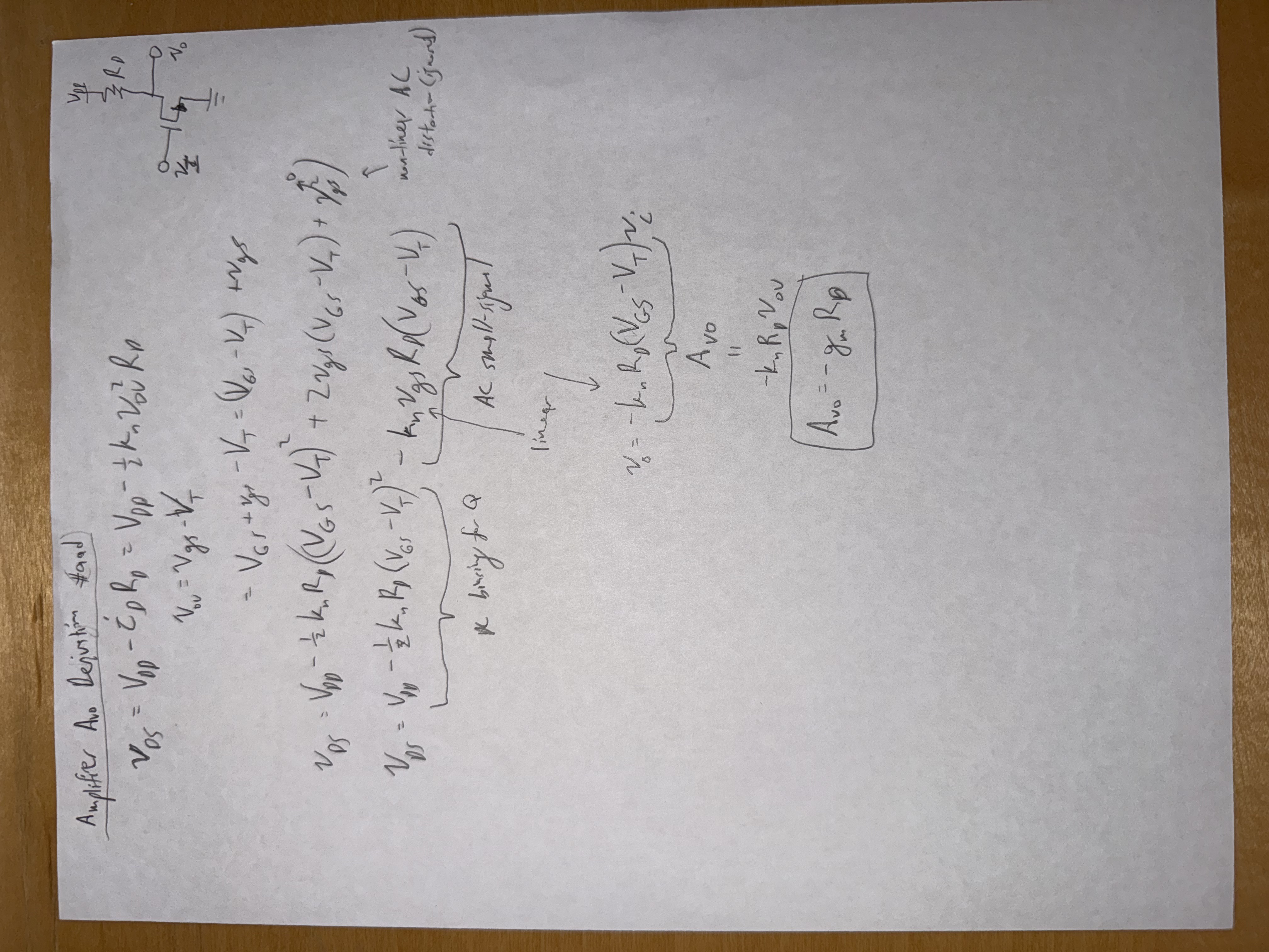
CD Amplifier
- Source follower because follows
-
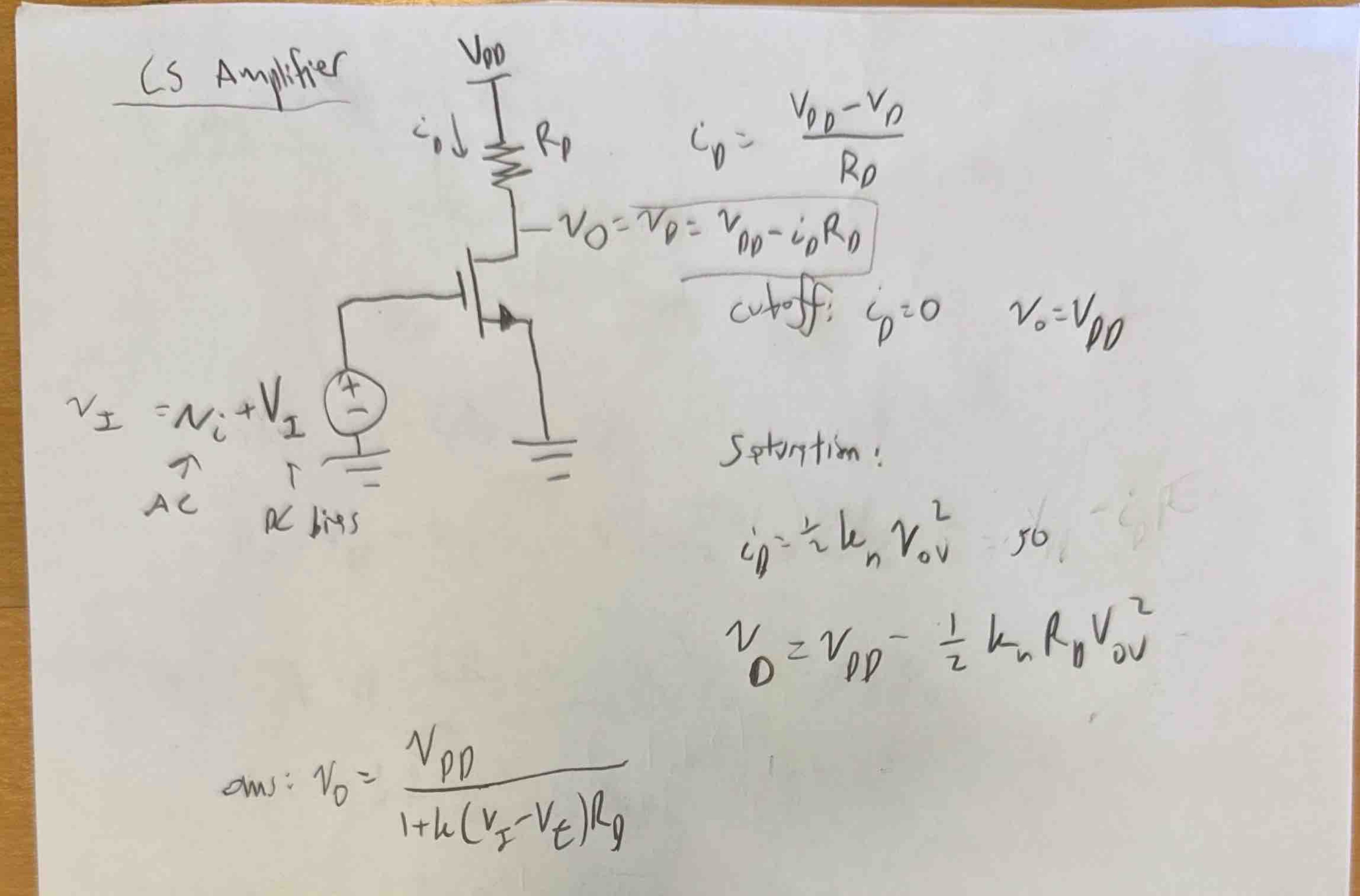
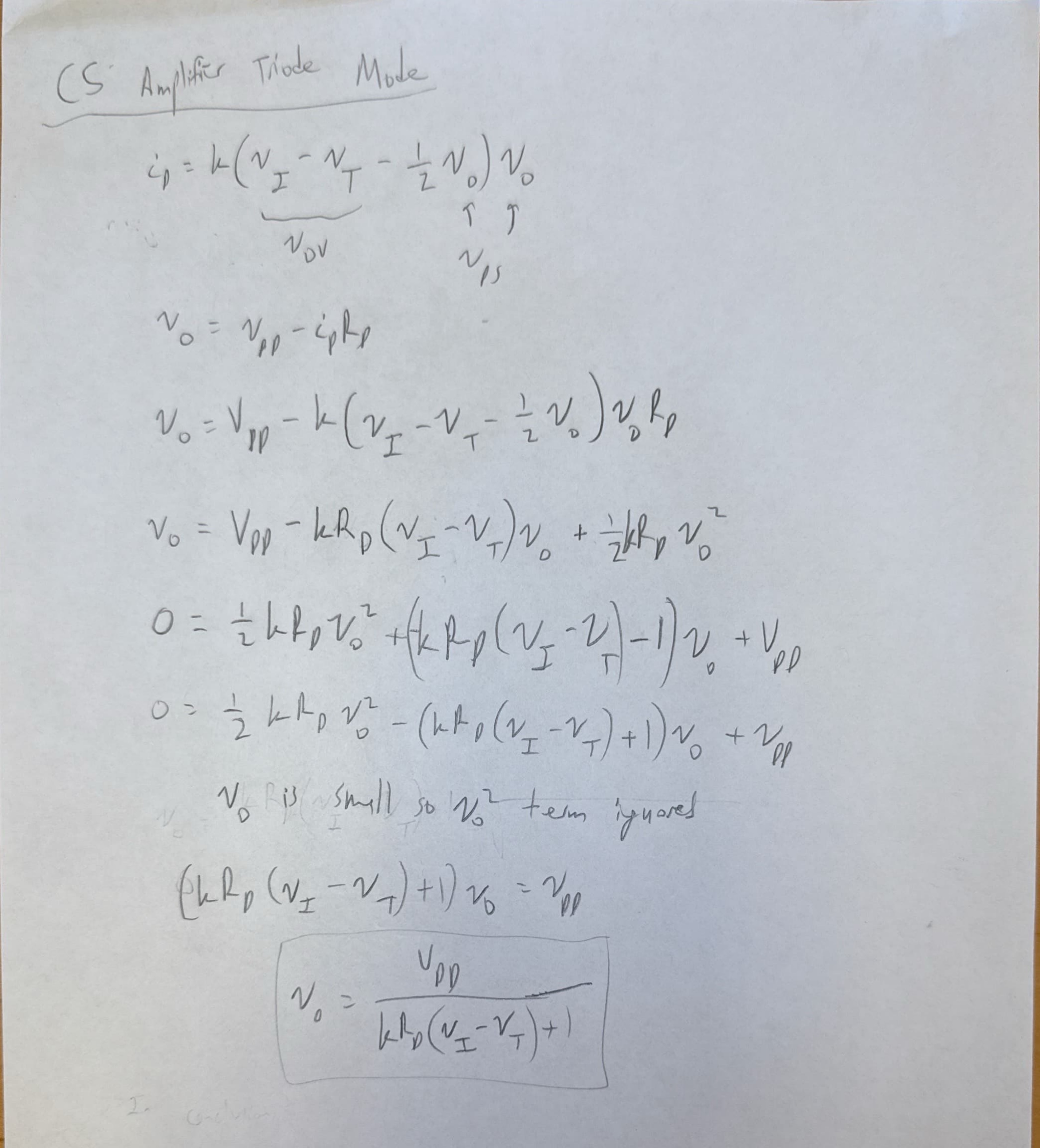
CS Amplifiers
-
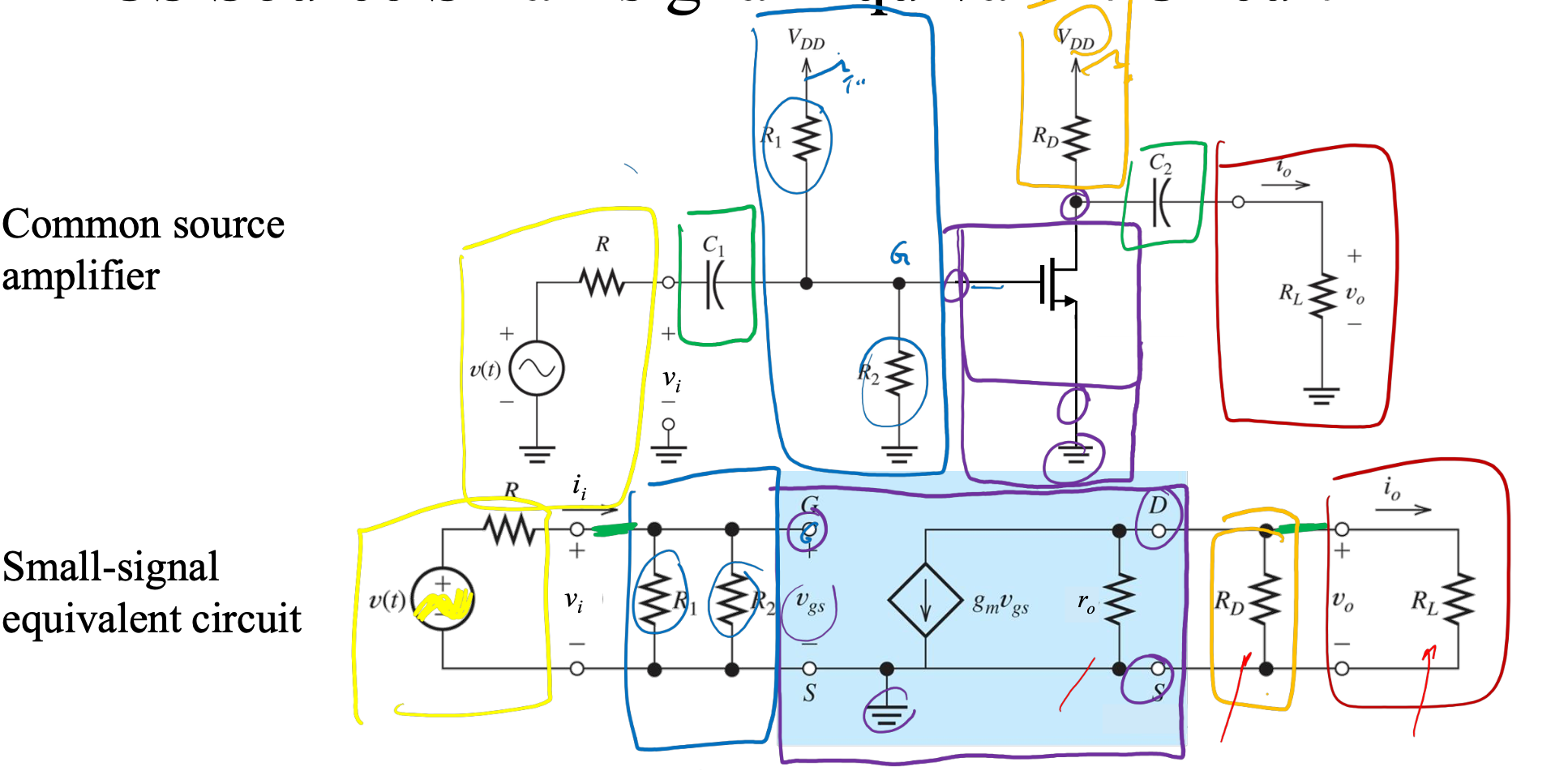
-
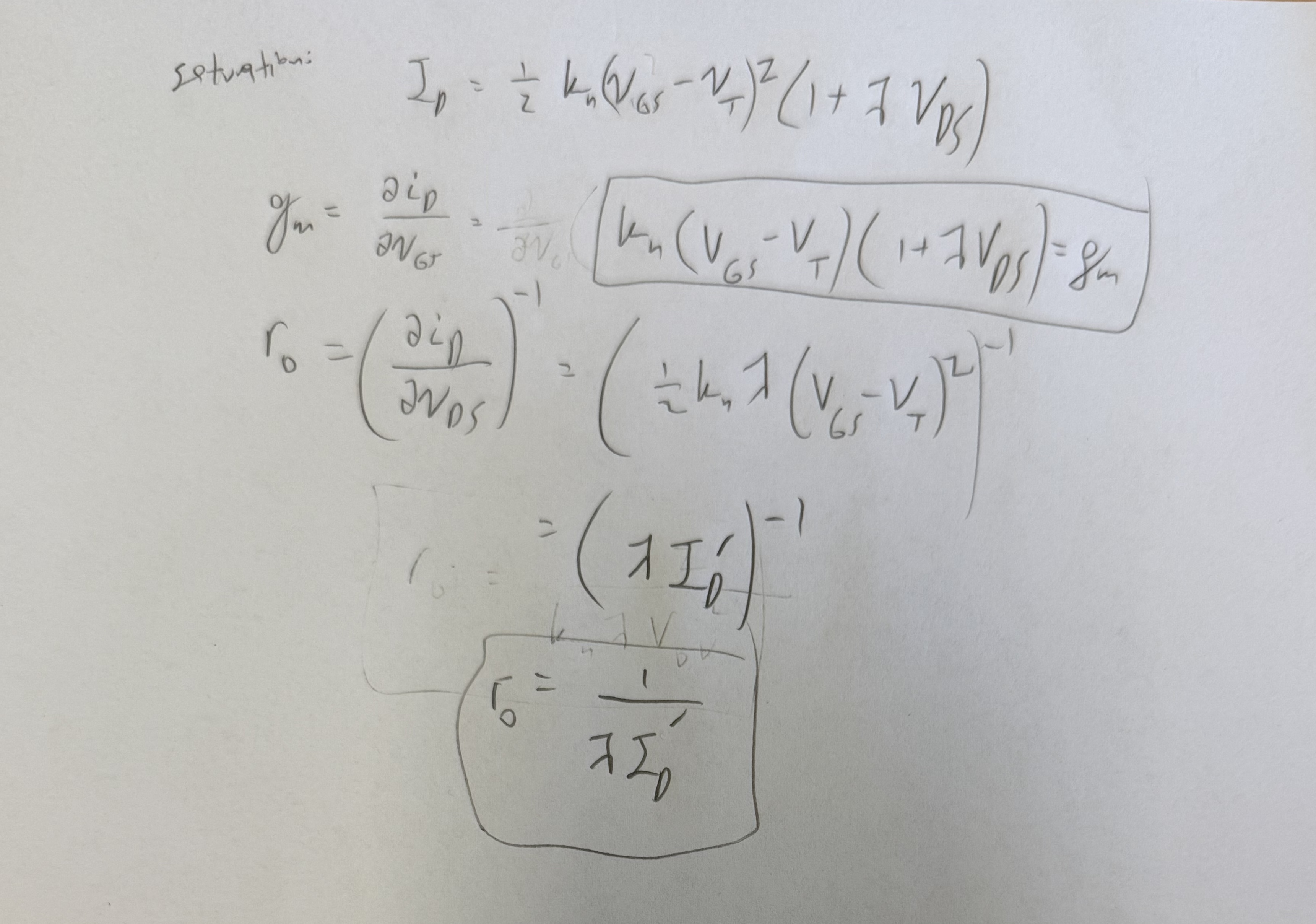
defines how leaky the transistor is due to channel-length modulation (increasing also increases ). See [[#How works]]. Without channel-length modulation (), is
-
models the voltage source's real-world imperfection (cannot supply infinite current)
-
Capacitors block out DC bias, just allowing the signal to pass through
-
-
Gain - is lower when there's a load resistance
- When no load resistance, open circuit gain
-
allows the output current to be converted into an output voltage
-
Early voltage is so meaning it's good if and are large because then the MOSFET is not very leaky
-
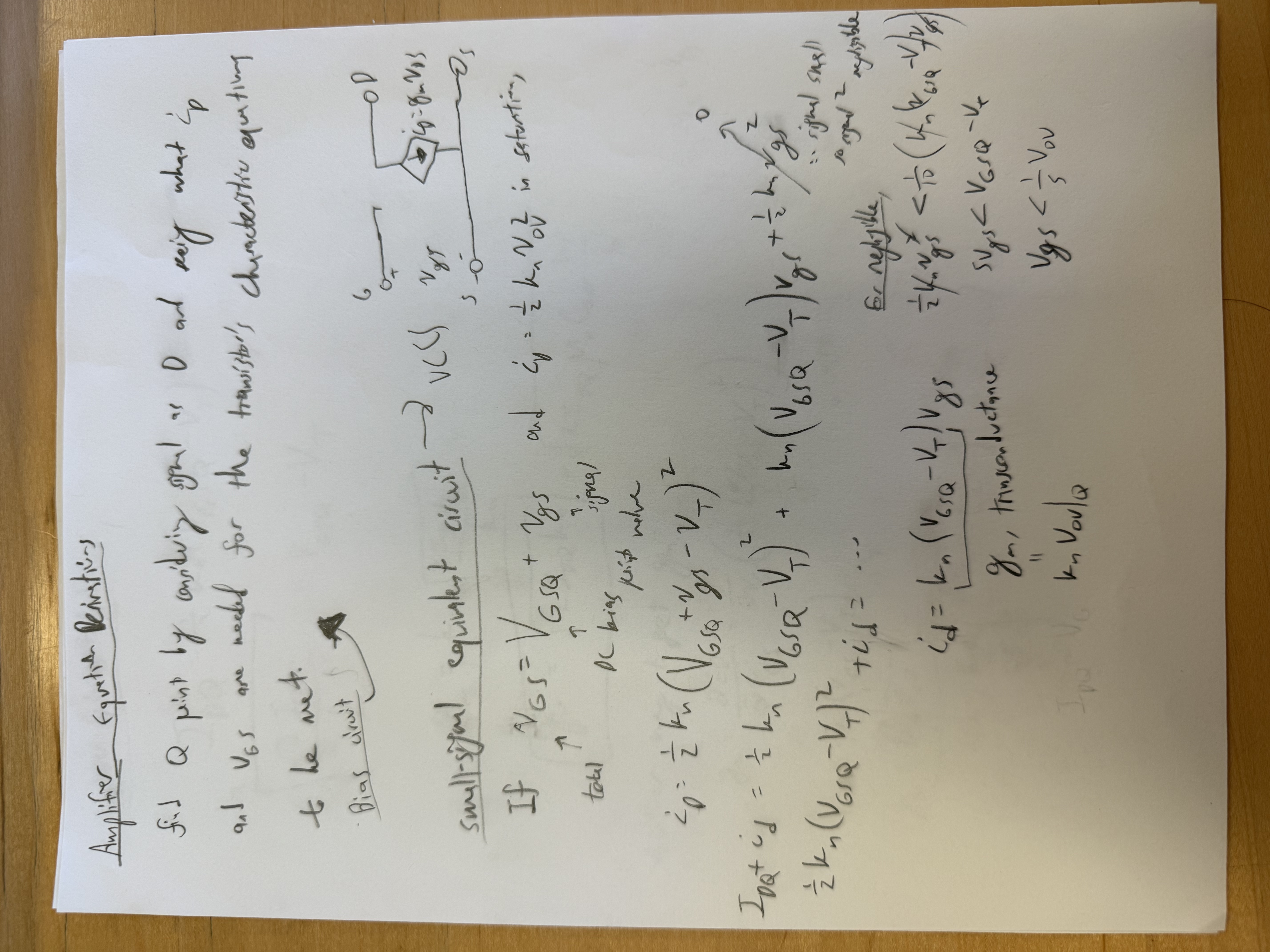
Bias circuit - the part of the circuit that sets the DC voltage so the transistor can operate in a small-signal linear region without distortion
-
Operating point - point at which load line (which describes all current-voltage pairs that the load constrains) matches the characteristic equation of the device
- Q-point - point at which signal voltage is 0 (quiescent as in dormant/inactive)
-
A VCCS is a transconductance amplifier
-
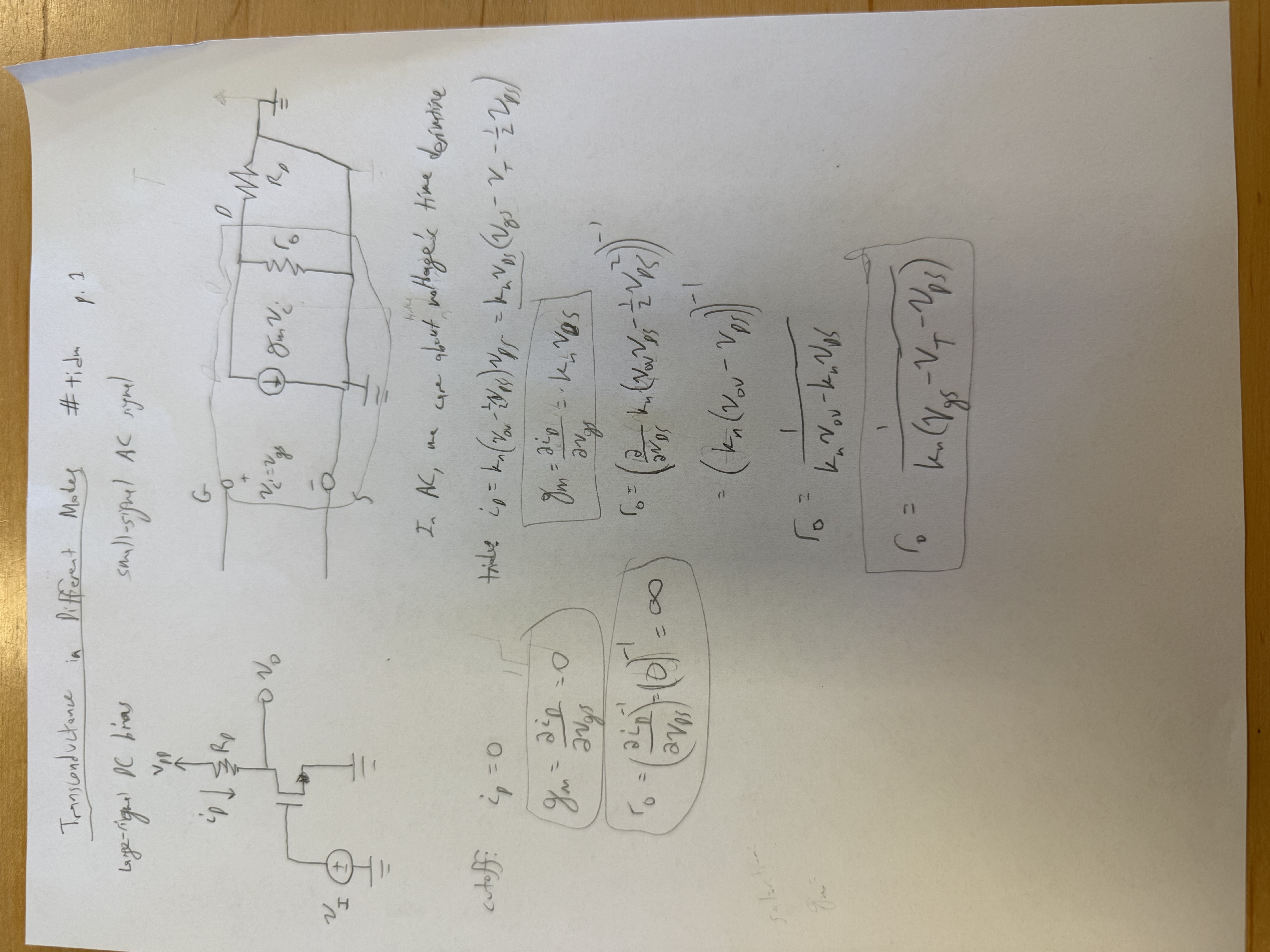
transconductance indicates how much changes for small changes in AKA . How much is transferred over.
-
Drain resistance
-
-
-
Graphs
-
voltage transfer characteristic (VTC) - graph
-
-
MOSFETs
-
MOSFET acts as a VCCS with a transconductance
-
Operate in saturation region for amplifiers and triode region for CMOS
-
CMOS - complementary MOS, manufacture nMOS and pMOS transistors on the same device
-
body is connected to source for both nMOS and pMOS
-
is for saturation
-
is for triode (variable resistor)
-
nMOS in enhancement-mode
-
transconductance - , how much the current output changes based on how the input voltage is modified
-
process transconductance
- mobility
-
-
when is negligible
-
-
called enhancement-type MOSFET because increasing above enhances the region's conductivity. For depletion-mode MOSFET, increasing above depletes the region (stops it from conducting).
-
where
-
Equations for the three regions (cutoff, triode, and saturation):
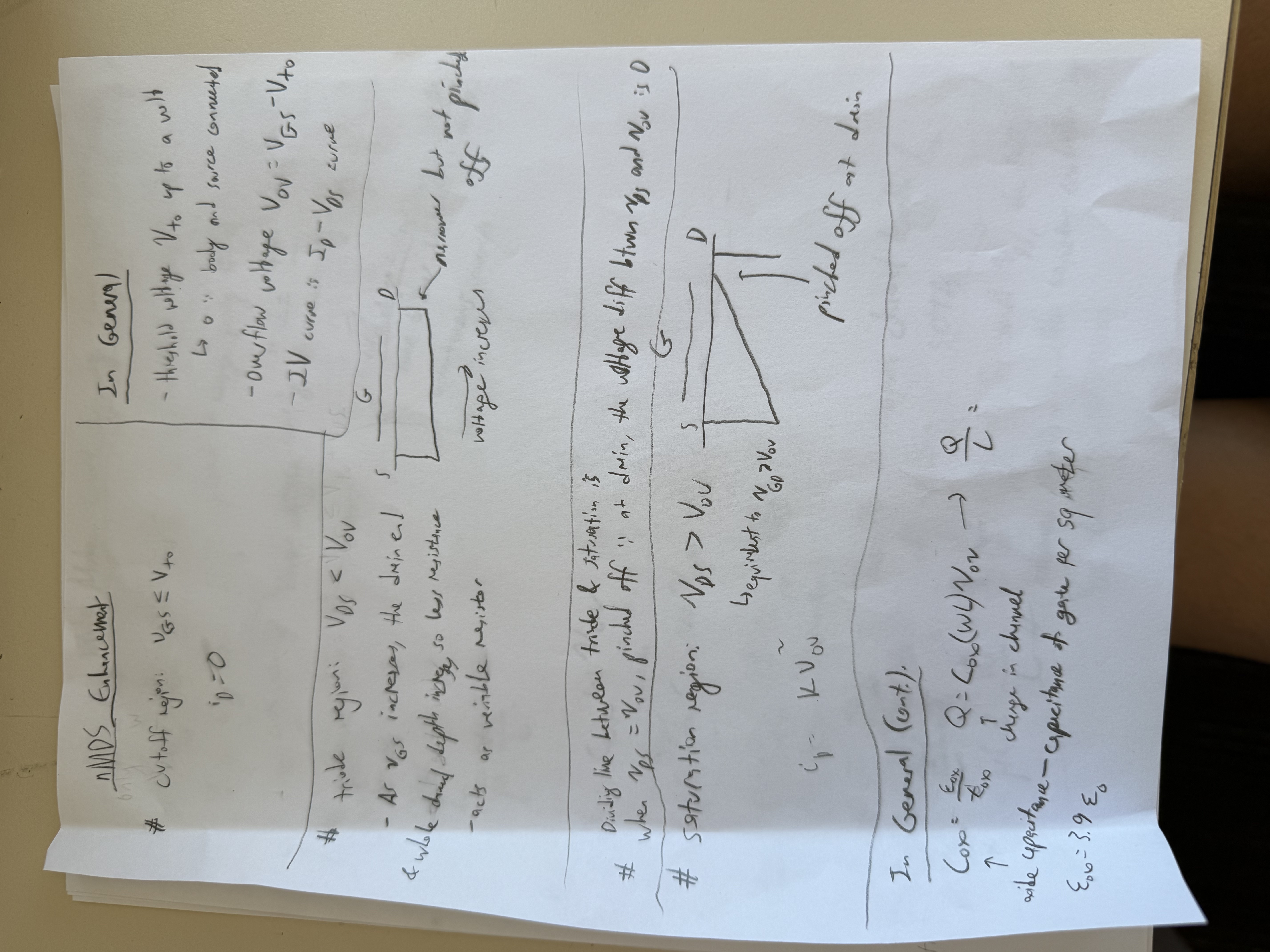
-
-
-
channel-length modulation occurs because as increases, the channel length changes, changing the current
-
-
-
Drift velocity where is the mobility
-
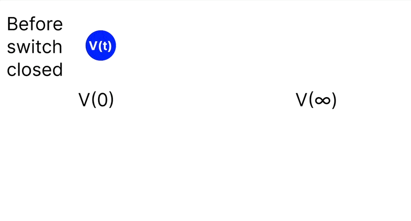
RC circuit (derivation at [[#RC Circuit]])
-
In general,
-
I interpret this as the first term being the permanent response and the second being the transient response due to the multiplier. Since a-b means to a from b, the sum is V(∞) + a vector that disappears with time that says go to V(0) from V(∞). Here it is animated:
-
-
Charging
-
-
Discharging
-
-
-
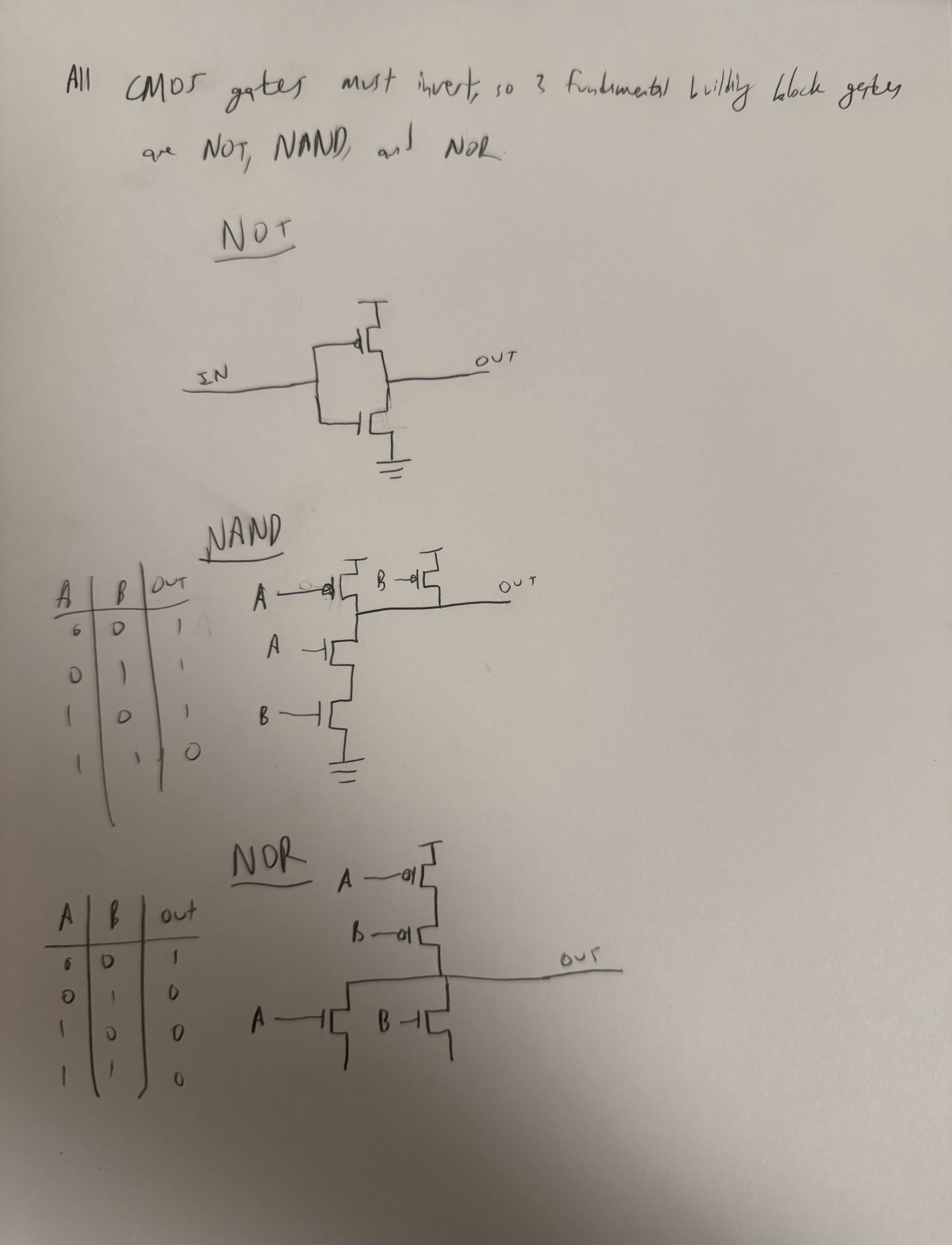
NOT, NAND, NOR Gates
- Tellegen's theorem - in an electrical network, sum of instantaneous powers in all branches is 0
-
Diode
-
Assuming
-
Assume that it is ON ( is reached). If we can show that there is a positive current through it, then there must be across the diode.
-
Assume that it is OFF. If we can show that there is a voltage across it greater than , then it must be ON.
-
-
Assume all OFF. When in parallel and choosing which one to turn ON, choose the one with lower
-
Models
-
ideal diode - V_f=0
-
constant voltage drop model
- FKA piecewise linear model - V_f=0.7
-
Shockley model
-
reverse bias model
-
-
Open circuit voltage, short circuit current
-
Ideal diode
-
Acts like an open circuit when voltage less than the forward voltage
-
Acts like a constant voltage source for voltages greater than the forward voltage
-
Ideal diode's forward voltage is 0V
-
-
p-n junction
- Depletion region
-
Silicon diode forward voltage - 0.7 V
-
Doping
-
P-type doping - Boron, adds a hole
-
N-type doping - Phosphorus, adds a free electron

-
-
-
High voltage is used in transmission because
-
High voltage means that the current goes down for the same power because
- A lower current means that the voltage drop between the generator and substation, , is smaller since the of the transmission line is constant and the decreases. The voltage drop across the transmission lines modeled as resistors went down even though the voltage on the line is higher. With a constant R and a lower current with HV, goes down and also goes down since V in the power equation measures the voltage drop, which went down.
-
-
Inductor
-
-
k - geometry
-
- permeability
-
A - cross-sectional area
-
N - # turns
-
-
Energy stored is
-
constant-current device
-
-
equivalent combinations like that of a resistor
-
Time constant
-
-
Capacitors
-
constant-voltage device
-
Voltage cannot change instantaneously on a capacitor (unless we do dirac delta functions)
-
-
- relative dielectric constant
-
- dielectric constant
-
- permittivity of free space (9E-12 F/m)
-
-
- C ∝ A and C ∝ 1/d
-
and
-
Types
-
Ceramic - cheap, low C
-
Polymer - HV
-
Electrolytic - polar, large C
-
Surface mount capacitors
-
IC capacitor
-
-
-
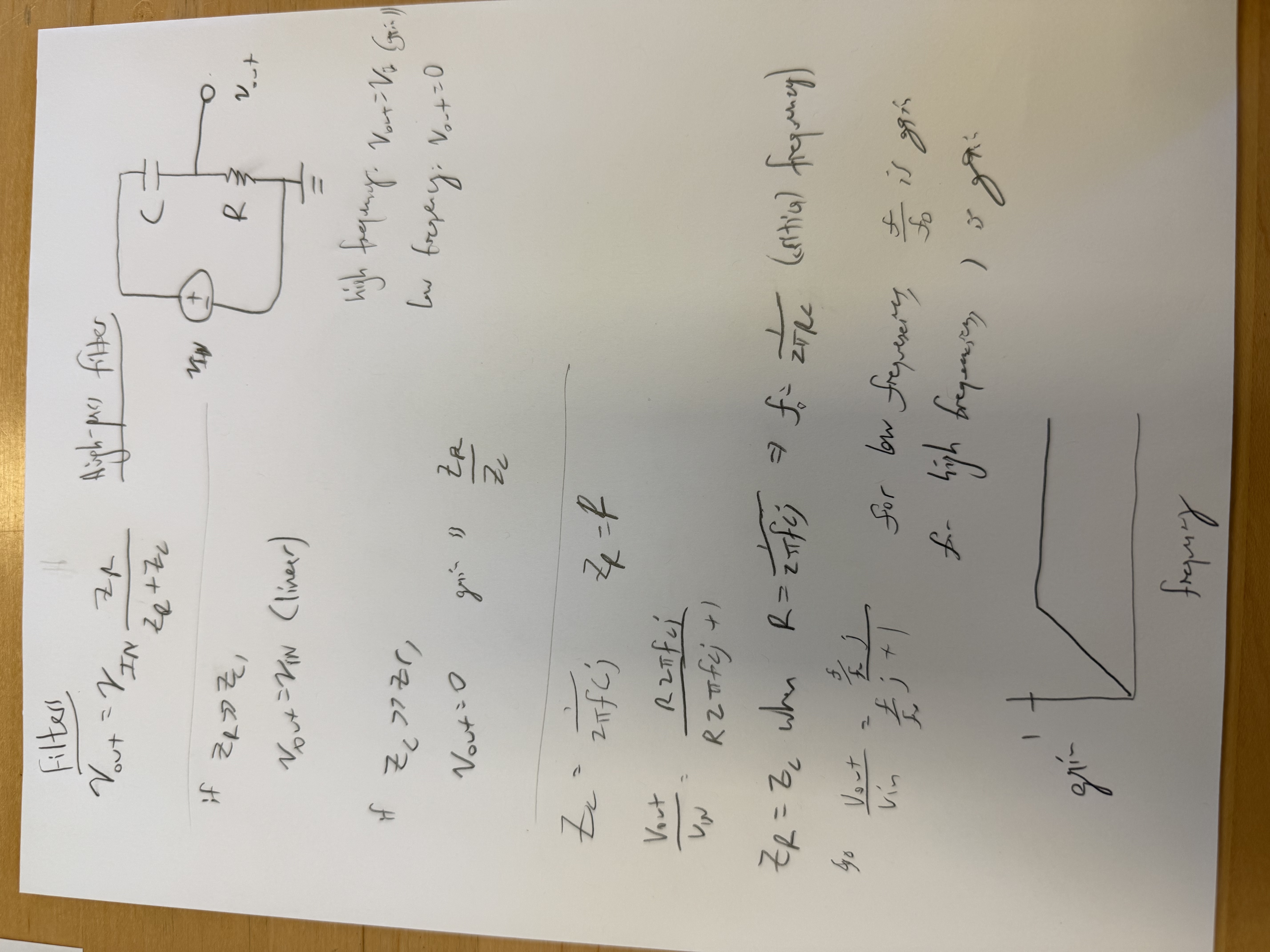
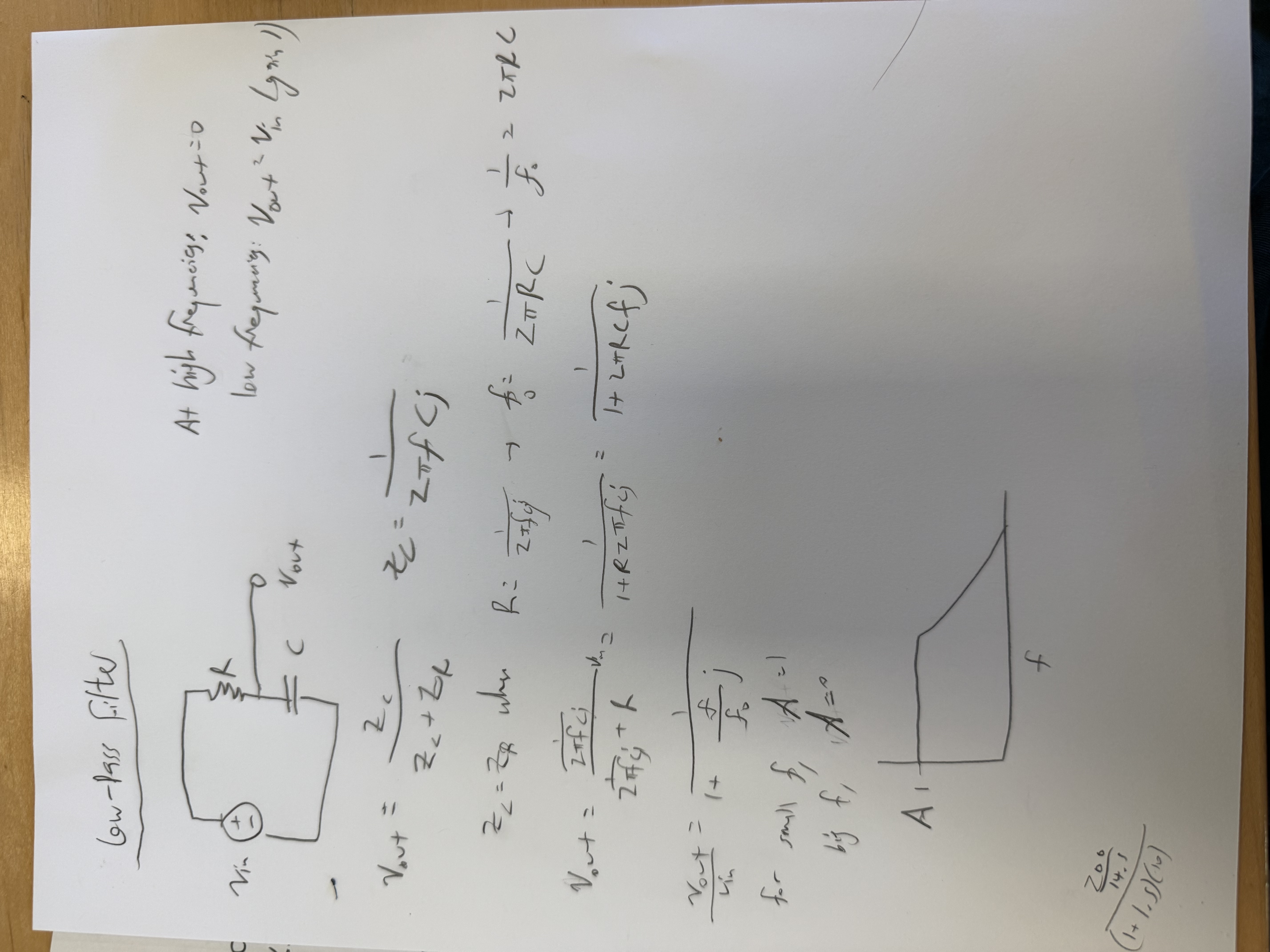
Waves
-
Nodal analysis: write out KCL (for nodes with unknown voltages) in terms of voltages
-
Full steps
-
Choose reference node and label the nodes' voltages. Use for unknown. Use voltage divider to find out relevant voltages if possible.
-
Label current directions
-
Apply KCL at all non-reference nodes (using Ohm's law integrated in the eqns)
-
-
-
Current divider ([[#Current Divider|derivation]])
-
. mn current ∝ inverse of %resistance in same component
- (special case of two resistors)
-
-
Voltage divider ([[#Voltage Divider|derivation]])
- . mn voltage ∝ %resistance in same component
-
Resistor Chart

-
Double-subscript notation:

-
Combination in series and parallel
-
Equivalent resistance for series resistors is sum because KVL means voltages add up and current is the same in series: becomes
-
Equivalent resistance for parallel resistors is the way it is because KCL means currents add up and voltages constant: becomes
-
These all have the same behavior for equivalent resistance/inductor:
- resistance
- inductance
-
Likewise, these all act the same (flipped, so in parallel they act like resistors would in series)
- conductance
- capacitance
-
Derivations
Op-Amp
Four Interchangeable Amplifier Types
Amplifier
Also,
Transconductance Expressed in More Ways
In saturation,

Transconductance in the 3 MOSFET Modes
in saturation
in triode
Amplifier
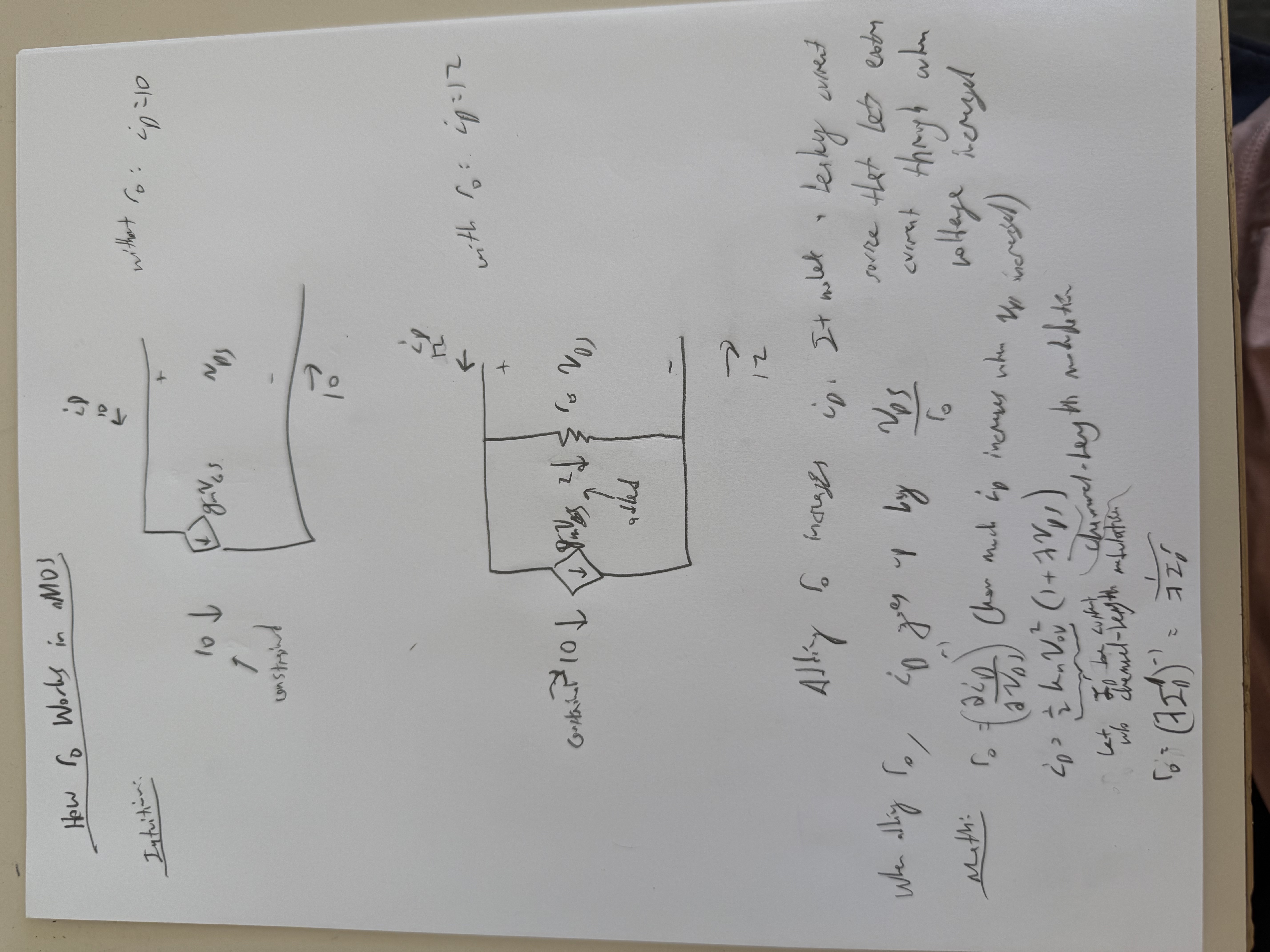
How works
o in is for "output" as in "output resistance" since it models the leakiness of a current source. For an ideal current source, increasing the voltage wouldn't affect how much the current source delivers. For a non-ideal leaky current source (which simulates), increasing voltage () also increases current output ().